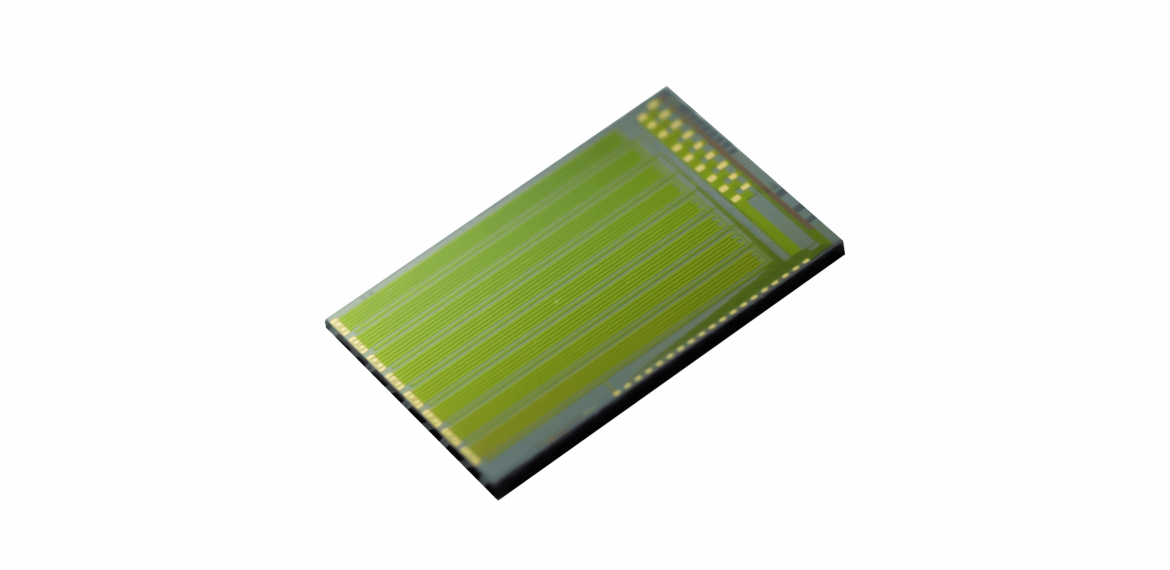
Hyperscale data centers are currently navigating a fundamental hardware transition to keep pace with the massive throughput required by artificial intelligence and distributed cloud clusters. In this landscape, the terminology often shifts between quantum computing and classical light-based processing, yet the B2B infrastructure of 2026 relies primarily on photonic chips to manage real-world traffic. Unlike quantum processors that manipulate subatomic states, these integrated optical circuits focus on the efficient transmission and modulation of light waves. By utilizing specialized TFLN chips, enterprises can achieve the 1.6T and 800G speeds necessary for modern networks without the cryogenic requirements of quantum systems. This distinction is vital for network architects selecting components that offer high reliability and low power consumption for immediate deployment.
Defining the Operational Scope of Photonic Chips
The primary function of photonic chips in the current information and communications sector is to manage high-speed data interconnects with minimal energy loss. These integrated circuits use light to carry information, bypassing the thermal and speed bottlenecks inherent in traditional silicon-based electronics. For mid- to long-reach solutions, the efficiency of a photonic chips platform is measured by its ability to integrate multiple optical functions—such as modulation and coupling—on a single substrate. By moving from bulk optics to chip-scale integration, manufacturers can provide more compact sub-assemblies for telecommunications and data center interconnects (DCI).
The Quantum Paradigm vs. High-Frequency Modulation
While quantum technology explores superposition and entanglement, the industrial focus remains on perfecting the electro-optic modulation used in 1.6T DR8 and 800G DR4 modules. Achieving these speeds requires photonic chips that can handle a 3dB-bandwidth of 70GHz while maintaining a half-wave voltage (Vπ) of less than 2V. This high-frequency performance is achieved through thin-film lithium niobate waveguides, which allow for faster switching than traditional photonic materials. These TFLN chips provide the high accuracy and low power consumption needed for system-level solutions, distinguishing them as a practical, high-performance alternative to experimental quantum architectures.
Industrial Infrastructure and TFLN Performance
Deploying a robust 1.6T or 800G link requires hardware that offers a DC-ER of over 25 dB and an insertion loss of less than 14 dB, including coupling loss. These metrics are the benchmarks for success in modern photonic chips design, ensuring that signal integrity is preserved across complex fiber-optic networks. Specialized TFLN chips support both differential and single-ended coupling, offering the flexibility required for automobiles, instruments, and wide-area communication. This versatility ensures that the hardware is ready for mass production, providing a scalable path for high-tech enterprises to meet the exponential growth of global data demand.
Conclusion
The evolution of digital infrastructure is increasingly dependent on the precision of integrated optical hardware. By utilizing thin-film lithium niobate technology, the industry can successfully navigate the complexities of 1.6T and 3.2T architectures. High-tech enterprises like Liobate are central to this progress, providing the specialized TFLN modulator chips and sub-assemblies needed to drive high-capacity optical modules. By establishing advanced platforms for PIC design, fabrication, and packaging, Liobate ensures that customers have access to the superior products and services required to scale the information and communications sector. As Liobate continues to refine its thin-film electro-optic technology, it remains a key contributor to the advancement of sustainable, high-speed connectivity.


